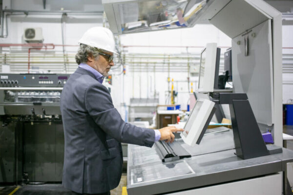
Erik Hosler Discusses AI for High-Precision Lithography in Advanced Nodes
The push toward smaller, more powerful semiconductor devices demand novel approaches to maintain precision during fabrication. One of the most critical processes impacted by this trend is lithography, where even slight inconsistencies can result in defective patterns or reduced device performance. Erik Hosler, a strong advocate for leveraging AI in precision lithography, emphasizes how integrating AI into lithography workflows can significantly improve accuracy, reduce errors and support the production of advanced nodes.
By leveraging artificial intelligence, manufacturers can enhance lithographic fidelity, reduce variability and optimize pattern transfer, making it possible to achieve higher yields in complex semiconductor designs.
The Role of AI in Lithography
Lithography, the process of patterning semiconductor wafers, becomes more complex as feature sizes decrease. The physical limits of light and material interactions increasingly challenge traditional lithographic methods. AI offers a solution by optimizing exposure parameters, predicting pattern distortions and compensating for variations during the patterning process.
By integrating machine learning models with lithography equipment, fabs can dynamically adjust settings to maintain precision. AI algorithms analyze real-time data from metrology systems, identifying deviations and suggesting corrective actions. This proactive approach reduces defects and maintains pattern integrity, even in highly intricate designs.
Achieving consistency in lithography also requires optimizing the interface between light sources and photoresist materials. AI-driven calibration techniques help maintain alignment between these elements, minimizing distortion and ensuring accurate pattern transfer. This capability is particularly valuable when dealing with high-density circuits where slight misalignments can result in functional failures.
Establishing feedback loops between lithography systems and AI-driven analysis platforms further improves precision. By continuously refining exposure algorithms based on real-time data, fabs can maintain consistency even when process conditions fluctuate.
Enhancing Resolution with AI-Driven Techniques
As nodes approach the 3nm scale, maintaining high resolution without introducing defects becomes a primary concern. AI enhances resolution by optimizing light source configurations and exposure patterns. By simulating how light interacts with photoresist layers, AI models predict optimal exposure settings that minimize distortion.
Maintaining consistent exposure quality in lithography requires adaptive techniques that can respond to minute variations. Erik Hosler adds, “Light source development and lithography advancements are shaping the future of semiconductor applications, where light will drive the next wave of innovation.” This highlights the importance of integrating advanced light management strategies to maintain precision in innovative semiconductor applications.
In addition to optimizing light exposure, AI can also enhance Optical Proximity Correction (OPC) techniques. By predicting how patterns can shift during exposure, AI algorithms help create mask designs that account for potential distortions, improving the accuracy of pattern transfer.
Advanced AI models can also predict how environmental changes within the lithography chamber affect exposure quality. By factoring in temperature variations and air flow disruptions, these models enable real-time adjustments that maintain pattern fidelity even in fluctuating conditions.
Real-Time Monitoring and Adjustment
Implementing AI for real-time lithographic adjustments can significantly improve yield rates. AI-driven monitoring systems detect variations during exposure and automatically adjust parameters to maintain consistency. This approach is particularly valuable in multi-patterning processes, where maintaining alignment across multiple exposures is crucial.
Integrating AI with metrology data also supports continuous improvement. By analyzing post-lithography inspection results, AI models refine exposure strategies, reducing the occurrence of common defects like line edge roughness or pattern collapse.
Real-time data fusion from multiple sensors can further enhance process control. By combining optical feedback with environmental monitoring, AI systems can detect subtle shifts that might impact pattern quality. This multi-layered analysis helps maintain high resolution throughout the lithographic process.
Developing multi-point monitoring systems that combine AI insights from various stages of lithography can further increase precision. By correlating data from exposure, etching and inspection phases, fabs can identify inconsistencies and fine-tune the entire patterning workflow.
Addressing Lithography Challenges with AI
One of the significant challenges in advanced node lithography is managing variability caused by environmental factors or material inconsistencies. AI helps mitigate these issues by correlating environmental data with lithographic outcomes. By identifying patterns between cleanroom conditions and defect rates, AI models suggest adjustments that stabilize the process.
Furthermore, integrating predictive maintenance algorithms with lithography equipment ensures that tools operate within optimal ranges. By forecasting when components may drift out of calibration, AI minimizes downtime and maintains high-quality output.
To further enhance stability, AI-driven vibration analysis can detect micro-movements that disrupt alignment during exposure. By proactively adjusting for these shifts, the system maintains pattern integrity, even when environmental vibrations are unavoidable.
Building robust maintenance frameworks that incorporate AI-driven diagnostics can help identify potential disruptions before they impact production. This proactive approach helps maintain continuous operation while reducing the likelihood of costly equipment failures.
The Future of AI-Driven Lithography
As AI models become more sophisticated, their ability to fine-tune lithography processes will continue to improve. Future developments may include AI-driven hybrid exposure techniques that combine multiple patterning strategies within a single lithographic pass. Such advancements will help maintain precision even as feature sizes continue to decrease.
Collaboration between AI developers, lithography tool manufacturers and semiconductor engineers will be vital for creating adaptable systems. By aligning AI capabilities with industry requirements, fabs can achieve higher precision and yield in advanced node production.
Exploring AI integration with in-situ monitoring tools could further enhance control. By embedding AI processors directly within lithography systems, fabs could achieve faster response times, allowing adjustments to occur without interrupting production.
Building Precision in Lithography with AI
Integrating AI into high-precision lithography is essential for sustaining innovation in semiconductor manufacturing. By automating adjustments and enhancing exposure accuracy, AI-driven approaches reduce variability and improve yield. As nodes continue to shrink, leveraging AI will be crucial for maintaining the quality and efficiency of advanced semiconductor devices.
Ongoing investment in AI research and collaboration between technology developers and fabs will ensure that lithography processes remain adaptable to future challenges. By fostering innovation in AI-driven lithography, the semiconductor industry can continue to meet the demands of next-generation device architectures.
Developing training programs to upskill fabrication technicians in AI-driven lithography techniques will also be essential. Ensuring that personnel understand how to interpret AI-generated insights and make data-driven decisions will help maintain consistent quality as lithography processes become more complex.
Investing in interdisciplinary collaboration between AI specialists and lithography engineers will further enhance process stability. By pooling expertise from both fields, fabs can develop more resilient lithography systems capable of maintaining high precision even as manufacturing demands increase.